¶ Overview
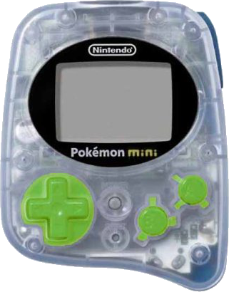
The Pokémon Mini was a handheld game system designed and manufactured by Nintendo, released in late 2001 (JP, NA) in three colors all with heavy Pokémon theming.
The system was powered by a single AAA battery, and was touted with a active playtime of around 60 hours. It is the smallest known system that features interchangeable game cartridges.
¶ Hardware Specifications
| CPU | Epson S1C88V20 (S1C88) 4MHz |
| Display | Monochrome 96x64 passive-matrix (SED1565) |
| Internal ROM | BIOS (4KiB) |
| Internal RAM | System RAM (4KiB) |
| Internal Storage | 8KiB I2C EEPROM (internal) |
| Cartridge | 8x21 bi-directional parallel bus |
| Unique Features | Rumble (pager motor), Shake sensor (reed switch) |
¶ Internal System Features
- External LCD parallel interface
- Internal fixed function drawing engine, with double-buffered frame copies
- Priority encoded interrupt engine
- 32 hardware IRQs (3 non-maskable)
- Up to 96 software IRQs
- 45 implemented in Pokémon mini BIOS
- 8x timers
- 6x General purpose
- One timer pair comparator is used for square wave audio generation
- Can operate in 16-bit mode, by enabling a count-through mode
- 1x 256hz timer
- 1x Second counter
- 6x General purpose
- System voltage monitor (ADC)
- 10-bit input port
- 8 pins are allocated to user inputs, with an additional two wired to cartridge connector for insertion detection and external interrupts
- Configurable de-jitter
- 8-bit general-purpose I/O port
¶ Memory Map
Internally, the Pokémon mini has 16mB of addressable space. The internal memory map overlaps the external memory map, resulting in a 8.25KiB section of the cartridge being normally inaccessible; however due to the cartridge only having 21 latched addressing bits and the address being fully decoded the otherwise unmapped rom can be accessed in the mirrored regions.
| Start Address | End Address | Description |
|---|---|---|
| 000000 | 000FFF | Internal System ROM |
| 001000 | 001FFF | Internal System RAM |
| 002000 | 0020FF | System Registers |
| 002100 | FFFFFF | External Bus |
¶ Internal System ROM (BIOS)
The internal system ROM consists of 4k of internal mask ROM. This provides functions for system initialization, configuration, LCD and power control. Additional functions are provided for direct access to special flash functions for Nintendo development cartridges, although no development hardware has been found. The bios provides 26 software interrupts in total, as described in the interrupt vector table.
¶ Internal System RAM
There are 4kB of total memory inside of the Pokémon mini, although a nearly a quarter of this memory is shared with the drawing engine. All parts of the drawing engine may be individually disabled, so with clever tricks it is possible to reclaim these sections for other uses.
| Start Address | End Address | Description |
|---|---|---|
| 1000 | 12FF | Display back-buffer |
| 1300 | 135F | Sprite attribute table |
| 1360 | 141F | Tile Map |
| 1420 | 14DF | Tile map extended (Mode 3 only) |
| 14E0 | 1FFF | General purpose |
¶ System Registers
All system control registers are mapped in a single 256 byte block. Only the registers which respond to reads / writes will assert the bus, unmapped values in this region will be left floating, resulting in bus capacitance leaving the last value asserted on the bus for a brief period of time.
|
Address |
Peripheral block |
Register Bits |
|||||||
|---|---|---|---|---|---|---|---|---|---|
|
7 |
6 |
5 |
4 |
3 |
2 |
1 |
0 |
||
|
00 |
System Control |
Start-up contrast |
CE1 |
CE0 |
|||||
|
01 |
|
|
|
|
|
|
|
|
|
|
02 |
|
|
|
|
CLKCHG |
OSCC |
VDC1 |
VDC0 |
|
|
08 |
Second Timer |
|
STRST |
STRUN |
|||||
|
09 |
STDL |
||||||||
|
0A |
STDM |
||||||||
|
0B |
STDH |
||||||||
|
10 |
System Voltage Monitor |
|
SVDDT |
SVDON |
SVDS |
||||
|
18 |
General Purpose Timer |
PRPRT1 |
PST1 |
PRPRT0 |
PST0 |
||||
|
19 |
|
|
|
|
PRTF1 |
PRTF0 |
|||
|
1A |
PRPRT3 |
PST3 |
PRPRT2 |
PST2 |
|||||
|
1B |
|
PRTF3 |
PRTF2 |
||||||
|
1C |
PRPRT5 |
PST5 |
PRPRT4 |
PST4 |
|||||
|
1D |
|
PRTF5 |
PRTF4 |
||||||
|
20 |
P03_04 |
P05_06 |
P07_08 |
P09_P10 |
|||||
|
21 |
P11_15 |
P19_20 |
P21_28 |
P29_31* |
|||||
|
22 |
|
P15_16 |
|||||||
|
23 |
E03 |
E04 |
E05 |
E06 |
E07 |
E08 |
E09 |
E10 |
|
|
24 |
|
E11 |
E12 |
E13 |
E14 |
E19 |
E20 |
||
|
25 |
E21 |
E22 |
E23 |
E24 |
E25 |
E26 |
E27 |
E28 |
|
|
26 |
E15 |
E16 |
E17* |
E18* |
|
E29 |
E30 |
E31 |
|
|
27 |
F03 |
F04 |
F05 |
F06 |
F07 |
F08 |
F09 |
F10 |
|
|
28 |
|
F11 |
F12 |
F13 |
F14 |
F19 |
F20 |
||
|
29 |
F21 |
F22 |
F23 |
F24 |
F25 |
F26 |
F27 |
F28 |
|
|
2A |
F15 |
F16 |
F17* |
F18* |
|
F29 |
F30 |
F31 |
|
|
30 |
General Purpose Timer |
MODE16_A |
|
PTOUT0 |
PTRUN0 |
PSET0 |
CKSEL0 |
||
|
31 |
|
PTOUT1 |
PTRUN1 |
PSET1 |
CKSEL1 |
||||
|
32 |
RDR0 |
||||||||
|
33 |
RDR1 |
||||||||
|
34 |
PTM0 |
||||||||
|
35 |
PTM1 |
||||||||
|
36 |
CDR0 |
||||||||
|
37 |
CDR1 |
||||||||
|
38 |
MODE16_B |
|
PTOUT2 |
PTRUN2 |
PSET2 |
CKSEL2 |
|||
|
39 |
|
PTOUT3 |
PTRUN3 |
PSET3 |
CKSEL3 |
||||
|
3A |
RDR2 |
||||||||
|
3B |
RDR3 |
||||||||
|
3C |
PTM2 |
||||||||
|
3D |
PTM3 |
||||||||
|
3E |
CDR2 |
||||||||
|
3F |
CDR3 |
||||||||
|
40 |
Clock Timer |
|
TMRST |
TMRUN |
|||||
|
41 |
TMD |
||||||||
|
44 |
Unknown Sub-System |
|
|
|
|
|
|
|
|
|
45 |
|
|
|
|
|
||||
|
46 |
|
|
|
|
|
|
|
|
|
|
47 |
|
|
|
|
|
||||
|
48 |
General Purpose Timer |
MODE16_C |
|
PTOUT4 |
PTRU4 |
PSET4 |
CKSEL4 |
||
|
49 |
|
PTOUT5 |
PTRUN5 |
PSET5 |
CKSEL5 |
||||
|
4A |
RDR4 |
||||||||
|
4B |
RDR5 |
||||||||
|
4C |
PTM4 |
||||||||
|
4D |
PTM5 |
||||||||
|
4E |
CDR4 |
||||||||
|
4F |
CDR5 |
||||||||
|
50 |
Inputs (K00~K11) |
KCP07 |
KCP07 |
KCP07 |
KCP07 |
KCP07 |
KCP07 |
KCP07 |
KCP00 |
|
51 |
|
KCP11 |
KCP10 |
||||||
|
52 |
K07D |
K06D |
K05D |
K04D |
K03D |
K02 |
K01D |
K00D |
|
|
53 |
|
K11D |
K10D |
||||||
|
54 |
|
CTK0H |
|
CTK0L |
|||||
|
55 |
|
CTK1L |
|||||||
|
60 |
General Purpose I/O |
IOC07 |
IOC06 |
IOC05 |
IOC04 |
IOC03 |
IOC02 |
IOC01 |
IOC00 |
|
61 |
P07 |
P06 |
P05 |
P04 |
P03 |
P02 |
P01 |
P00 |
|
|
62 |
Impedance / Pull-up control ? |
|
|||||||
|
70 |
Output Control |
|
|
|
|||||
|
71 |
|
|
|
||||||
|
80 |
Drawing engine |
|
MAPSIZ |
ENACOPY |
ENASPR |
ENAMAP |
INVMAP |
||
|
81 |
FRAMECNT |
FRAMEDIV |
LCDINIT |
||||||
|
82 |
MAPBASEL |
|
|||||||
|
83 |
MAPBASEM |
||||||||
|
84 |
|
MAPBASEH |
|||||||
|
85 |
|
MAPSCX |
|||||||
|
86 |
|
MAPSCY |
|||||||
|
87 |
SPRBASEL |
|
|||||||
|
88 |
SPRBASEM |
||||||||
|
89 |
|
SPRBASEH |
|||||||
|
8A |
|
LINECNT |
|||||||
|
8B |
Unknown |
This area reads back 0x00, it's purpose is unknown as of this moment. Personal intuition assumes it is used for rendering circuit in microcode |
|||||||
|
8C |
|||||||||
|
8D |
|||||||||
|
8E |
|||||||||
|
8F |
|||||||||
|
F0 |
|||||||||
|
F1 |
|||||||||
|
F2 |
|||||||||
|
F3 |
|||||||||
|
F4 |
|||||||||
|
F5 |
|||||||||
|
F6 |
|||||||||
|
F7 |
|||||||||
|
FE |
LCDCTRL |
||||||||
|
FF |
LCDDATA |
||||||||